4X1 Mux Logic Diagram - Plc Program To Implement 4 1 Multiplexer Sanfoundry : Circuit diagram of a 2:1 mux using transmission gate logic.. Isnt a mux a logic gate already? 2:1 mux verilog in data flow model is given below. You need a combinational logic with 16 input pins, 4 select lines and one output. 4:1 mux structural representation with 2x1 muxes. The logic circuit and symbol of 2x1 mux is shown in figure 2.
For the logic diagrams in this application note, the programmable lut codes are shown in red. Do you mean how do you make a 4x1 mux out of 2x1 muxes? How to write 4x1 mux in vhdl xilinx. Multiplexers, or mux's, can be either digital circuits made from high speed logic gates used to switch digital or binary data or they can be analogue types using transistors 4 channel multiplexer using logic gates. We can analyze it y = x'.1 + x.0 = x' it is not gate using 2:1 mux.
What Is Multiplexer How It Works Multiplexer Circuit from circuitdigest.com 4 to 1 multiplexer, multiplexer in digital logic, 4 to 1 multiplexer in hindi multiplexer tutorial, 4:1 multiplexer, multiplexer and. The truth table of 4x1 mux is : Multiplexer can act as universal combinational circuit. Simplified block diagram of the 4 1 multiplexer circuit. Source code:module fa_mux(sum,cout,a,b,cin);output cout,sum;input a,b,cin;wire cinb;mux m1(.z(sum),.d0(cin),.d1(cinb),.d2(cinb),.d3(cin),.s0(a),.s1(b) documents. Design truth table,logical expression,circuit diagram for it. The diagram belowshows how with only 1 rfid reader and 4 x mux4x1 can cover a big surface. As we know a multiplexer has 1 output and 2n where n is the no.
Mux working symbol and logic diagram.
Out std_logic_vector (0 to 3)); The logic for the complete multiplexer is shown in figure 3 where the two mux4_cells are combined together with the internal muxf7 multiplexer. I have this program i am suppose to make for this diagram 4x2 decoder diagram: We can easily understand the operation of the above circuit. In std_logic_vector (0 to 7); Write a vhdl code to implement 4 x 1 mux using logic gates, if else and with select and simulate the design. Here, the transmission gates selects. Now, this circuit shows we need two 4x1 multiplexer has four data inputs i 3, i 2, i 1 & i 0, two selection lines s 1 & s 0 and one output y. We can analyze it y = x'.1 + x.0 = x' it is not gate using 2:1 mux. Multiplexer (mux) 2 x 1mux design watch more videos at www.tutorialspoint.com/videotutorials/index.htm lecture by: Circuit diagram of a 2:1 mux using transmission gate logic. You need a combinational logic with 16 input pins, 4 select lines and one output. As we know a multiplexer has 1 output and 2n where n is the no.
8 1 mux logic diagram exclusive wiring diagram design. In std_logic_vector (0 to 7); The logic for the complete multiplexer is shown in figure 3 where the two mux4_cells are combined together with the internal muxf7 multiplexer. 4:1 mux structural representation with 2x1 muxes. A multiplexer can be designed using various logics.
Analog Switches Multiplexers Can Share Resources Digikey from www.digikey.com Multiplexers and de multiplexers examradar. Multiplexer can act as universal combinational circuit. Write a vhdl code to implement 4 x 1 mux using logic gates, if else and with select and simulate the design. 4 1 multiplexer 40gbps centellax ms4s1v1m agilent n4983a. We can analyze it y = x'.1 + x.0 = x' it is not gate using 2:1 mux. As far as i know we can make a 16:1 mux using five 4:1 mux. I made it be an xor but you can change the 0 and 1 bits on the data inputs (in00, in01, in10, in11) and make it do whatever. Multiplexer circuits 2 1 and 4 1.
In this post, i will tell you what is multiplexer (mux) and i am also will tell you about its working with logic diagram and uses.
Multiplexer can act as universal combinational circuit. How to make 8x1 multiplexer using 2 4x1 multiplexer? 2:1 mux verilog in data flow model is given below. The truth table of 4x1 mux is : Design truth table,logical expression,circuit diagram for it. If you will write down the logic equations for a 4 to 1 multiplexor, then the logic will become obvious. Derive the truth table that defines the required relationship problem 7: Write a vhdl code to implement 4 x 1 mux using logic gates, if else and with select and simulate the design. Simplified block diagram of the 4 1 multiplexer circuit. Hello, can someone please explain me how to design a logic circuit of 4x1 mux using 2x1 muxes and logic gates ? Do you mean how do you make a 4x1 mux out of 2x1 muxes? A multiplexer can be designed using various logics. 4x1 mux schematic symbol figure 6(b):
Pardon my crappy diagram but i hope you get the solution! The implementation of not gate is done using n selection lines. Design truth table,logical expression,circuit diagram for it. Complete the timing diagram (note that qa and qb are initially low (0)). How to make 8x1 multiplexer using 2 4x1 multiplexer?
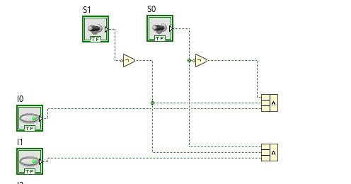
4x1 Multiplexer Design In Labview Tutorial 33 from microcontrollerslab.com I keep trying to change the initial values of the output array from 0 to 1 and 1 to 0 by just negating them but i still never get the desired result. Verilog program not getting desired output on 4x1 mux. Write a vhdl code to implement 4 x 1 mux using logic gates, if else and with select and simulate the design. · pc with windows xp. I made it be an xor but you can change the 0 and 1 bits on the data inputs (in00, in01, in10, in11) and make it do whatever. 4 1 multiplexer 40gbps centellax ms4s1v1m agilent n4983a. 8 bit adder module adder(s,cout,a,b,cin); Multiplexers different ways to implement verilog by examples.
Pardon my crappy diagram but i hope you get the solution!
The diagram belowshows how with only 1 rfid reader and 4 x mux4x1 can cover a big surface. I made it be an xor but you can change the 0 and 1 bits on the data inputs (in00, in01, in10, in11) and make it do whatever. When sel is at logic 0 out=i0 and when select is at logic 1 out=i1. Implement a full adder with two 4 x 1 multiplexers. How to write 4x1 mux in vhdl xilinx. Complete the timing diagram (note that qa and qb are initially low (0)). I keep trying to change the initial values of the output array from 0 to 1 and 1 to 0 by just negating them but i still never get the desired result. Architecture demux_archi of demux14 is begin process (i,s) begin case s is when 00 => o(0)<= i. Derive the truth table that defines the required relationship problem 7: The 4 1 multiplexer logic diagram will likely be your initial step to creating and placing your very first community, and you will also come across that it's going to be quite a bit cheaper than likely out to. 4 1 multiplexer 40gbps centellax ms4s1v1m agilent n4983a. In std_logic_vector (0 to 7); 4x1 mux schematic symbol figure 6(b):